Making Your Own Printed Circuit Boards
Ilan Mandel
What is a printed Circuit Board?

Types of PCBs
Single Sided
Double Sided
Multi-layer
Flexible PCBs
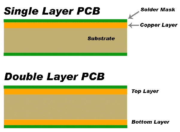
Anatomy of a PCB
read more at Autodesk
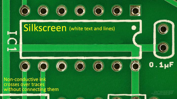
Silkscreen
The very top and bottom layer of your board inclues:
Layer 21-22: tPlace/bPlace
Layer 25-26: tNames/bNames
pcbgogo
Soldermask

Bantam Tools
Top
This is the top copper routing layer of the board

Pads
Layer 17: These inclue the annular ring for through hole pads

Vias
Layer 18: Vias are used for passing a signal between layers of a board


Dimension
Layer 20: Specifies the board outline

Bottom
Layer 16: Specifies the bottom copper traces

Unrouted
Layer 19: "air wires" show routes from your schematic that have not yet been drawn on your board

Board Design Tips
- Leave enough spacing for assembly
- Orient parts in the same direction
- No 90º bends in routes
- Ground planes are your friend
- Perpendicular traces across layers


Power Considerations
- Separate power and control ground as much as possible
- If you need to make traces wider here is a calculator
- Separate analog and digital ground/traces